
Introduction
Few people today remember the times before the internet and the ubiquity of semiconductor electronics. Yet only a few decades have passed. The next iteration of our civilization, based on artificial intelligence, is emerging before our eyes.
Few know that the foundation of this revolution was a surprising discovery made by a Pole in 1916. Jan Czochralski from Kcynia is the creator of the so-called Czochralski method for producing single crystals. This inexpensive and brilliantly simple method, applied in the mid-20th century to the production of silicon single crystals, provided the impetus for the tremendous development of electronics.
And it all began like this…
An Astonishing Accident
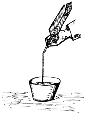
In 1916, Jan Czochralski, a Polish chemist working in the Berlin laboratory of the AEG electrical company, made an accidental discovery that changed the course of history. Exhausted from research aimed at finding a method to measure the crystallization rate of metals, Czochralski made a seemingly trivial mistake. Intending to record his observations, he instinctively dipped his pen not into an inkwell but into a nearby crucible of molten tin. To his surprise, when he withdrew the pen, a thin thread of solidified metal hung from the nib. This unexpected appearance of a metal thread intrigued him. He repeated the action, dipping the nib into the molten tin and slowly withdrawing it. He observed the formation of another thread. When he pulled the pen out faster, the thread was shorter. A series of systematic experiments conducted that evening confirmed that the speed at which the pen was withdrawn from the molten metal affected the length and structure of the solidified thread. He realized that this phenomenon could provide key insights into the crystallization properties of metals.
Czochralski noted that the notch in the pen’s nib acted like an open capillary; crystallization in capillary tubes had previously been described by Gustav Tammann. The Polish scientist thus replaced the pen with a glass tube and the hand with a clockwork mechanism. This allowed him to control the speed of pulling the crystalline thread.
This accidental experiment, later named the Czochralski method and first published in 1918, marked a breakthrough in the technology for producing single crystals essential for semiconductor electronics.
In 1950, across the Atlantic, American scientist Gordon Teal struggled with the challenge of obtaining large, high-quality germanium single crystals for transistors. It turned out that the Czochralski method, used in metallurgical laboratories, was suitable for this purpose after necessary improvements. Later, Teal applied the method to produce silicon crystals. Without the Czochralski method, the development of microprocessors, computers, mobile phones, and many other devices would have been impossible. The simplicity and versatility of the method made it the foundation of the technological revolution, securing its place in laboratories and electronics companies worldwide.

Jan Czochralski, born in 1885 in Kcynia, in a Poland divided by partitions, was a self-taught chemist who rose to the heights of science. Despite lacking formal higher education, he worked in Berlin’s chemical and metallurgical industries, leading the metals laboratory at AEG. His accidental discovery in 1916 was not merely a stroke of luck but a testament to his abilities and scientific rigor. After returning to Poland in 1928, he became a professor at the Warsaw University of Technology. Unfortunately, in 1945, he was not allowed to return to the university for reasons that remain unclear. He spent his final years in Kcynia, running a small chemical plant called BION. He died in 1953. It was not until 2011 that the Warsaw University of Technology officially recognized his contributions, lifting the infamy imposed decades earlier.
Czochralski named his crystallization rate measurement method the “capillary method” (Capillarverfahren, Capillarmethode), referring to the initial suction of molten material through a capillary at the end of a hook. The first description of the method, titled “Ein neues Verfahren zur Messung der Kristallisationgeschwindigkeit der Metalle” (“A New Method for Measuring the Crystallization Rate of Metals”), was published in the journal Zeitschrift für physikalische Chemie in 1918. The manuscript was received by the editors on August 19, 1916—a date considered the birth of the method. The publication detailed the technical aspects and results of initial experiments on tin, zinc, and lead.
The natural consequence of this discovery was the application of the “crystallization rate measurement method” to the production of single crystals. As early as August 1918, Hans Joachim von Wartenberg used this method to obtain zinc crystals, being the first to replace the capillary with a crystal seed. Further modifications were proposed by, among others, Ervin von Gomperz (1922), H. Mark and collaborators (1923), and E.G. Linder (1925).
Method
The essence of the Czochralski method is simple. The material to be crystallized is melted in a crucible, and a capillary or a pre-prepared seed is introduced into the surface layer of the melt. After drawing a small amount of metal, crystallization begins, and the seed is pulled at an appropriate speed to maintain contact with the molten substance. Surface tension holds the column of liquid material at the capillary’s outlet or “attached” to the seed. The contact of this column with cooler air causes it to solidify slowly above the liquid surface, resulting in a single crystal with an ordered atomic structure.
The Czochralski method has many advantages:
- The direction of crystal growth is determined by the orientation of the seed,
- The lack of contact with the crucible ensures stress-free growth,
- It allows for easy control of quality and chemical composition, including doping,
- A defective crystal can be fully or partially remelted, reducing material waste and costs,
- Large crystals can be obtained under various conditions, including in specific gas atmospheres.
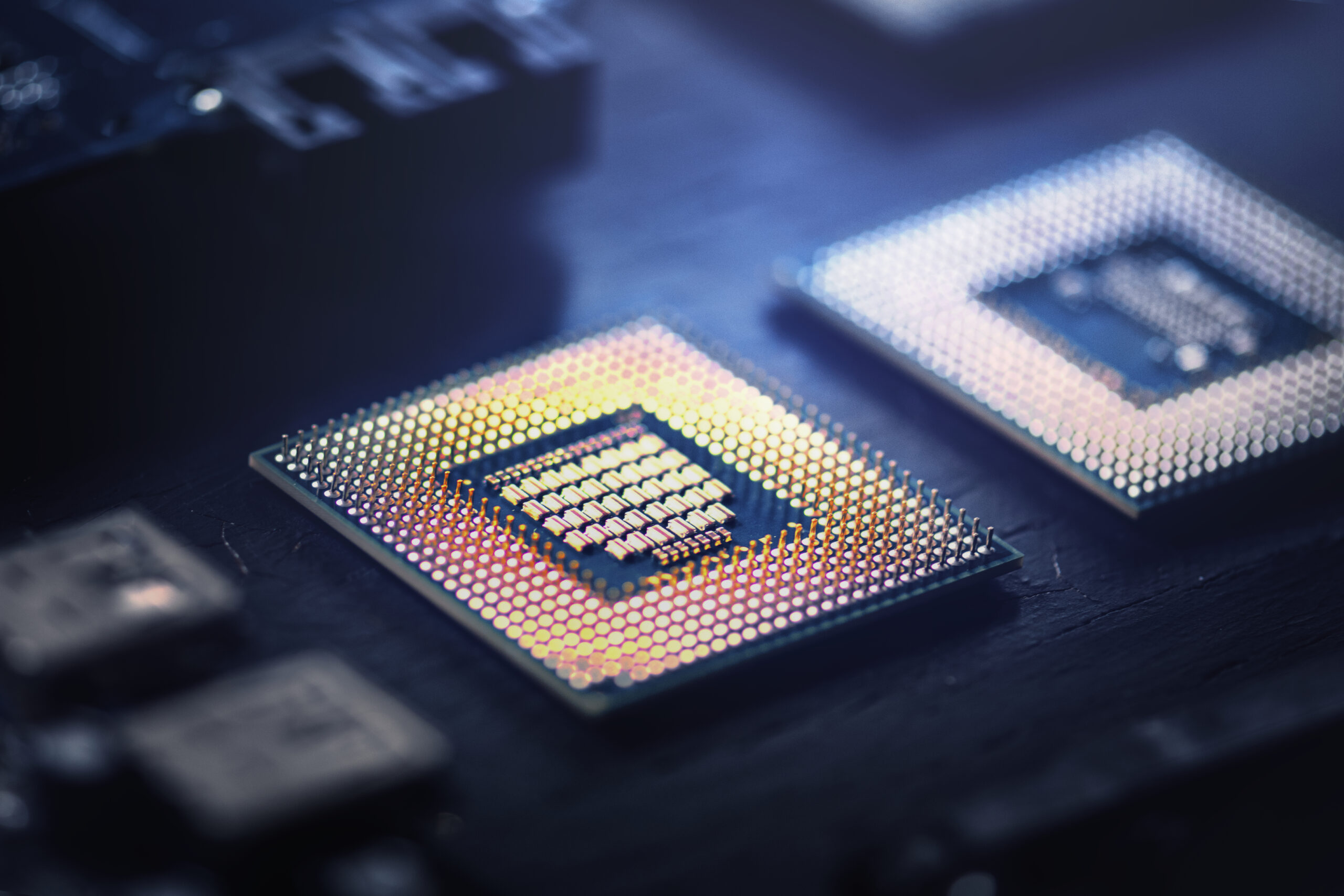
Initially, the method was used only for producing metal single crystals. However, it quickly found application in producing single crystals of many other materials, including silicon, which is critical for electronics. No other crystal growth method can compare to it.
Jan Czochralski did not patent his invention and did not gain financial benefits from it. He likely never imagined that he would become, in a sense, the “father of silicon electronics.” It was precisely thanks to his discovery that the development of high-quality transistors and modern semiconductor technologies became possible.
Today
Jan Czochralski started with thin tin single crystals just 15 cm long. The first silicon crystals were about 2.5 cm in diameter and weighed only 50–200 grams. It was soon realized that growing larger crystals, from which wafers enabling the placement of multiple integrated circuits could be made, was more cost-effective. Increasing the diameter has significant economic importance: a 20 cm wafer can yield 74 64 Mb microprocessors, while a 30 cm wafer can produce 170 1 Gb processors.
The scale of the method’s development is evident in today’s silicon single crystal parameters—the primary raw material for integrated circuits. They can reach lengths of up to two meters, a diameter of 30 cm, and a weight of over 250 kg (such crystals have been produced by Wacker-Siltronic GmbH in Freiberg near Dresden since 2002). By 2006, over half of production was already using 30 cm wafers. It is also possible to produce silicon with a diameter of 45 cm and a weight of about 800 kg, though the costs and technology of producing such large crystals pose significant economic challenges.
Currently, about 99% of all semiconductor devices are made from silicon single crystals, with approximately 95% of crystals produced using various variants of the Czochralski process. Factories operate dozens of large-scale installations.
For decades, few knew who the creator of the “Czochralski method” was, and it was only in the 1980s that efforts began to restore the memory of this outstanding Polish scientist.
In the documentary film The Return of the Chemist, Professor Zbigniew T. Kuźnicki emphasized that Jan Czochralski belongs to the trio of the greatest Polish scientists, alongside Nicolaus Copernicus and Marie Skłodowska-Curie. The order can be determined by their impact on daily life—and here, as Kuźnicki noted, Jan Czochralski takes the lead.
Contrary to the expectations of optimists, silicon will remain the primary material for electronics for a long time, and with it, the Czochralski method will continue to be needed and used.